XEIA3 model 2016

XEIA3 model 2016
The INDUSEM is a new model of a scanning electron microscope intended for industrial applications. The system is based on a platform of the third generation of VEGA SEMs built-in a robust frame. This compact and transportable device equipped with an extra large chamber enables wide sample range for quality control and failure analysis within production plant.
With the new XEIA3 model 2016, TESCAN delivers not only an instrument top of its class, but also fulfils its commitment to continue helping researchers push science and development forward. This is also reflected in the careful customisation of every system in order to meet the specific needs of every customer. From materials to life sciences or from engineering to the semiconductor industry, TESCAN guarantees high-performance systems without any compromises.
Key Features
- A unique combination of a three-lens objective and crossover-free mode
- Advanced and variable detection system for simultaneous acquisition of various signals
- Sub-nanometre resolution: 0.7 nm at 15 keV
- Ultimate ultra-high resolution: 1 nm at 1 keV
- Angle-selective BSE detection for maximum topographical and elemental contrast at low energies
- Real-time In-Flight Beam Tracing™ for performance and beam optimisation
- Traditional TESCAN Wide Field Optics™ design offering a variety of working and display modes
- Efficient thermal power dissipation for excellent electron column stability
- New Schottky FE gun now enables beam currents up to 400 nA and rapid beam energy changes
- Ideal solution for inspection of the latest technology nodes in advanced failure analysis processes
- Ideal for imaging delicate biological specimens
- Imaging of magnetic samples possible
- Optimised column geometry makes analysis (SEM inspection and FIB nanomachining) of up to 8” wafers possible
- Unique live stereoscopic imaging using 3D Beam Technology
- User-friendly, sophisticated SW modules and automatic procedures
Xe plasma FIB key features
- Extremely powerful Xe plasma ion source FIB column for accomplishing even the most challenging large-scale milling tasks in unbeatably short time-frames.
- Versatile ion beam current range:
– high currents for cross-sectioning in TSVs, BGAs, and MEMS
– medium currents for large-area surface polishing and large-volume FIB tomography
– low currents for TEM lamella polishing, delayering, TOF-SIMS
– ultra-low currents for very fine polishing, nanopatterning and ion imaging - Large-mass xenon ions for ultra-high sputtering yields without any gas-assisted enhancement
- Large-scale 3D microstructural analysis
- Significant reduction in ion implantation at high voltages compared to Ga LMIS FIBs
- No intermetallic compounds formed during FIB milling
- Ideal for 3D ultra-structural studies of biological specimens such as tissue and whole cells via FIB-SEM
Applications
Semiconductors and Microelectronics
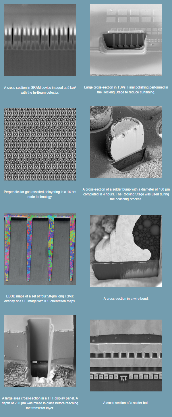
XEIA3 model 2016 is the ideal FIB-SEM system to satisfy the growing demand for ultimate resolution at low beam energies and large-scale FIB-SEM analysis. XEIA3 enables the imaging of beam-sensitive structures such as photoresists and ultra-thin transistor layers in the latest technology nodes. XEIA3 model 2016 is the system of choice for failure analysis in packaging technologies such as TSVs, BGAs and wire bonding that requires the milling of large volumes in the order of hundreds of microns in any dimension.
- Failure analysis in advanced packaging in:
– Trough silicon vias (TSV) analysis: cross-sectioning for analysis of stress levels and Cu intrusion, microstructure and grain distribution, examination of voids, cracks, delamination
– Ball grid arrays (BGA)
– Wire bonding - Failure analysis in integrated circuits that includes:
– Planar top-down gas-assisted delayering
– TEM lamella preparation
– Cross-sectioning - Circuit editing by means of deposition of conducting materials or insulators and FIB-cutting
- Failure analysis in MEMS – Microelectromechanical Systems
- FIB-SEM tomography for structural analysis in Cu pillar, TSVs, wires, ICs
- Solar cell inspection and efficiency analysis
- In-situ TEM lamellae imaging: STEM analysis and TKD-EBSD
- Large wafer inspection and micromachining
- Imaging of delicate photoresists
- EBIC fault isolation tests
- TOF-SIMS analysis in the battery industry
Material Sciences
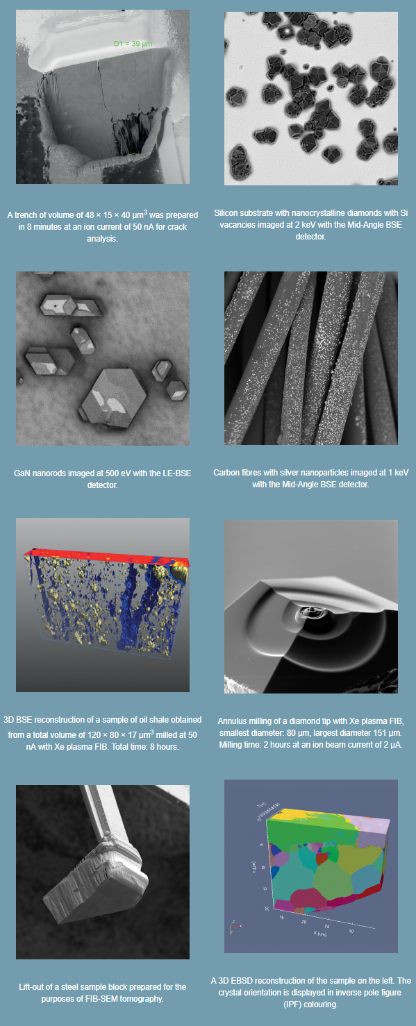
XEIA3 model 2016 is the ideal solution for imaging non-conductive materials such as ceramics and polymers and in general, all sorts of beam-sensitive samples. In terms of micromachining, Xe plasma FIB offers great advantages for the research and development in materials science that require site-specific removal of large volumes of material in a controlled way with high spatial resolution. Plasma FIB enables fast artefact and damage free milling without delamination, smearing, grain modification or other defects that are commonly introduced when using other sectioning techniques such as microtomes or mechanical polishing. In terms of microanalysis, xenon – in contrast to gallium – is inert and non-electrically active. It therefore does not form intermetallic compounds that might modify the original physical (electrical, magnetic) properties of the sample or interfere with elemental analyses.
- Study of samples with complex topography with ultimate resolution and enhanced depth of focus
- Imaging of magnetic samples
- Large-scale cross-sectioning for:
– Fatigue and crack formation analysis in the metallurgy, construction, automotive and aeronautic industries
– Phase analysis of metallurgical processes - FIB-SEM tomography:
– 3D EDX and 3D EBSD for quality tests in the wire industry
– 3D BSE for the characterisation of different phases in materials
– 3D analysis of porous and granular materials - In combination with TOF-SIMS:
– High-resolution microanalysis and surface characterisation of thin layers and coatings with minimal sample damage
– Identification of isotopes and species with similar nominal mass in nuclear research - Controlled ion implantation and doping of materials
- Fabrication of structures without Ga contamination such as plasmonic antennas
Life Sciences
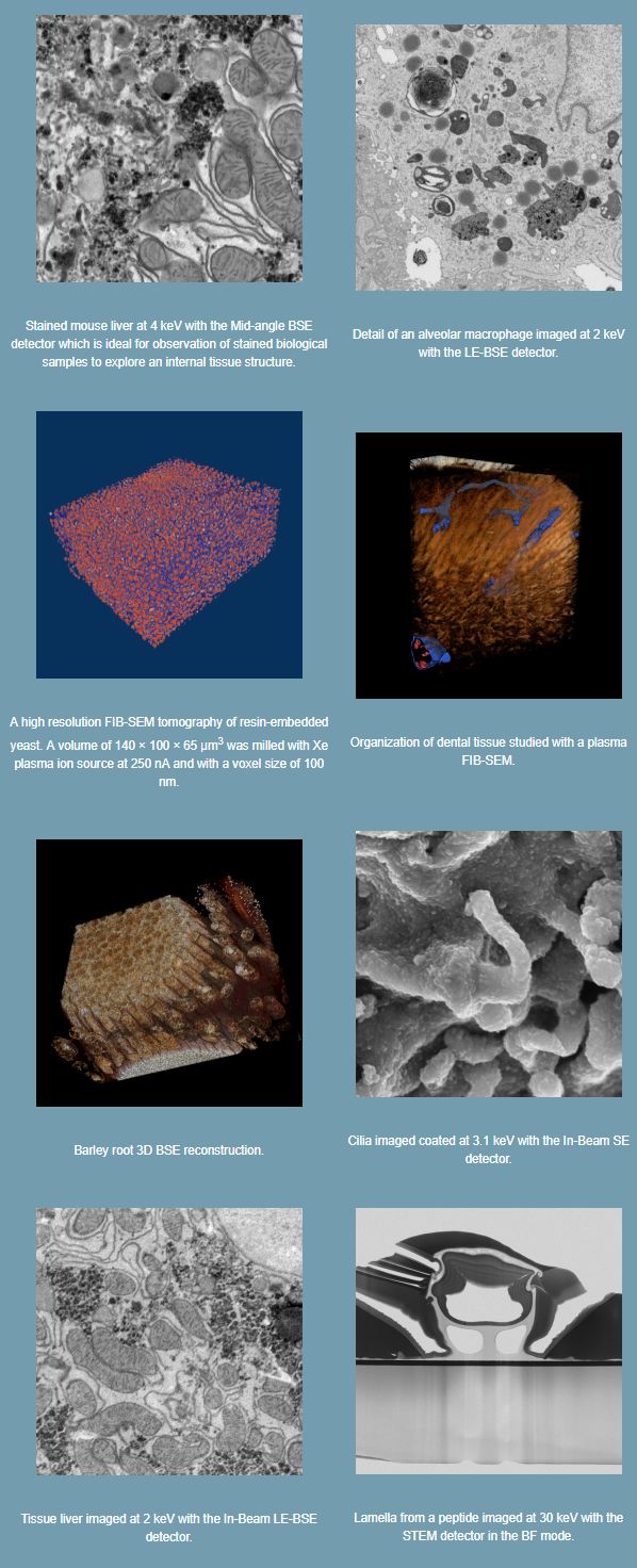
The ultimate resolution achieved by XEIA3 model 2016 at low beam energies is suited for imaging beam-sensitive biological specimens in their natural uncoated state. This represents a great advantage in terms of throughput and productivity as sensitive samples can be imaged without time-consuming sample preparation or fixation. Furthermore, the integration of Xe plasma FIB in SEM extends the role of electron and ion microscopy in life sciences. FIB cross-sectioning and FIB-SEM tomography of whole biological samples have become feasible only thanks to plasma FIB. Such sample analyses reveal localised morphological and structural information that cannot be obtained by other conventional imaging techniques. Some of the main applications of XEIA3 model 2016 in life sciences include:
- Imaging of cells and tissues in their natural uncoated state at low and ultra-low beam energies for maximum ultra-structural information and surface sensitivity
- Preparation of high-quality TEM lamellae
- FIB-SEM tomography of large sections of resin-embedded tissue and cells (brain, internal organs, yeast, plant roots)
- Research in cell biology: cross-sectioning of whole cells and tissue (human egg cells)
- Analysis of 3D ultra- and nano-structures of microfossils
- Preparation of TEM lamellae of large sections of biological samples (cells, tissue, grains, seeds)
- Sublayer analysis in large and hard-to-cut samples such as teeth, bones, dental implant interfaces
- Enhanced detection limits of light elements for high-resolution surface analysis of biological samples by means of the unique combination of plasma FIB and TOF-SIMS