
HAXPES-Lab
HAXPES-Lab
At a Glance
- Hard X-rays at 9.25 keV opens a window for bulk-sensitive photoemission
- Superior analyser performance in HAXPES by the market leader in the field
- Complete stand-alone home-lab solution
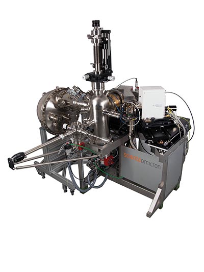
HAXPES-Lab is designed to allow hard X-ray photoelectron spectroscopy (HAXPES) measurements in standard lab environments. The instrument offers the unique possibility to investigate bulk properties of various materials, analyse buried interfaces and access deep core levels. HAXPES-Lab is a convenient to use, turnkey UHV system which includes a 9.25 keV monochromated Ga Liquid Metal X-ray Source and a EW4000 energy analyser allowing for analysis in the full kinetic energy range up to 9252 eV.
Photoelectron spectroscopy is an ideal tool to probe the chemical state of a material and as such it is becoming ever more required to investigate electronic structures of various solid materials in the bulk, on surfaces as well as at buried interfaces. A home laboratory facility that probes bulk and buried interfaces has up until now not been commercially available.
UPS and XPS have been available and highly accessible in decades. Both these techniques are surface sensitive and thus the field of photoemission has been regarded as a surface science technique. The development of the field of HAXPES, mainly at large synchrotron facilities, changed the field of photoemission to include the study of bulk properties. The HAXPES technique has become valuable and provided new insights into the properties of materials. As a consequence the beamlines providing HAXPES is popular and heavily booked. As of now the technique is also available in your laboratory.
Bulk-sensitive photoemission spectroscopy as a home laboratory experiment

The inelastic mean free path (IMFP) of photoelectrons for photon energies above 1000 eV increases with the kinetic electron energy roughly as Ekin0.78. This allows a significantly higher information depth of photoelectron spectroscopy in the hard X-ray regime (HAXPES) compared, e.g., to rather surface sensitive laboratory-based XPS systems using Al Kα excitation (hν = 1487 eV). HAXPES therefore provides the possibility to access the chemical information from the bulk of a material.
System outline and instrumental features

We have developed a unique lab system utilizing a monochromatized Ga-metal jet technique which provides a photon energy of hν = 9.25 keV. Thus it becomes possible to bring the bulk sensitive HAXPES technique from the synchrotron into the home laboratory.The HAXPES-Lab is mounted on a rigid bench frame with an ultra small floor-level foot-print. The bench includes suitable support facilities for the EW4000 analyser and alignment of the monochromatic Ga Liquid Metal X-ray source. The control system Mistral is included to control all parts of the system.This home laboratory system opens up possibilities for HAXPES measurements on a regular basis, making measurement time not limited to the valuable time at synchrotrons worldwide.
Ga liquid metal source

The high intensity monochromatized Ga Kα X-ray source at 9.25 keV consists of a liquid Ga anode and an ellipsoidal Si monochromator crystal. The liquid Ga anode is realized via the well proven Excillum Metal Jet technique, in which 70 kV electrons impinge on a high pressure jet of molten Ga alloy.
EW4000 high kinetic energy electron analyzer

The EW4000 energy analyzer is an extreme wide angle lens spectrometer featuring 60 degrees acceptance angle in both transmission and angular mode. The unit can be operated in fixed mode where a spectrum can be recorded within seconds by taking a snap shot of the detector image, covering 8% of the pass energy. The high voltage electronics provides ultra-stable conditions for reliable accurate measurements. Electron detection is featured by a modern 2-D low noise digital CCD-MCP detector system with a noise level of < 0.01 cps/channel.
For further details of the EW4000 analyser click this link
First proof of principal measurements

First results with the HAXPES-Lab prototype system have been acquired on Au and Si samples to show the capabilities of the new product.
3D Animation

Key applications for HAXPES-Lab
 HAXPES provides a larger information depth and the possibility to access the chemical information from the bulk of the material, which was utilized in several recent experiments at synchrotron beamlines, including the investigation of:
- Buried Interfaces in layered material stacks and future devices, e.g. solar cells, resistive switches, batteries
- Real-world samples, which describes specimen which cannot undergo any surface cleaning procedures or extra preparations. Photoemission measurements can be performed through potential surface contamination.
- In operando devices. For the development of future nanotechnology devices it is favorable to determine the chemical states of active layers below a top electrode. Working devices can be switched and measured in operando.
With Scienta Omicron’s HAXPES-Lab it becomes possible to perform these experiments in the home laboratory without the need to apply for synchrotron beam-times.
Core set-up includes:
- Ga Kα liquid metal jet X-ray source:
– Photon energy hν = 9252 eV - Focussing X-ray monochromator:
– Resolution ΔE < 1 eV
– Power up to 200 W on 50 μm spot - HAXPES analyzer EW4000:
– Angular acceptance ± 30°
– Resolution ΔE < 100 meV @ 10 keV
– 40 mm working distance
– 2D MCP/CCD detector - Analysis chamber
- Manipulator:
– 4-axis (x/y/z, polar rotation)
– PBN heating (up to 1170 K)
– Omicron flag style sample transfer - Control system:
– MISTRAL system control
– SES measurement software
Optional modules are available:
- Preparations facilities
- Al Kα source
- Sample transfer
- Glove box
- MBE
- etc.
 HAXPES-Lab